FR

We design,
simulate, and characterize
your power and analog
electronics.

From the first schematic to a production-ready board, for space, defense, and industrial systems.

From schematic
to characterized prototype.

A full-stack approach to power and analog electronics, from the first sketch on a notepad to a fully characterized, production-ready board. With proprietary tooling built in-house.

01

From Concept to Industrial Prototype

End-to-end product development. We turn an idea into a fully functional, production-ready board, schematic, layout, BOM, characterization.

  • Feasibility studies & concept assessment
  • Schematic capture & PCB design
  • Component selection, sourcing & BOM
  • Functional mock-ups & early prototypes
  • Iterative characterization & refinement
  • DfT, DfM, DfX for scalable production
02

Technical Documentation & Compliance

Auditable, traceable documentation that supports every line of your design, from prototype to qualification. We comply with applicable standards without overclaiming.

  • Standards-compliant design & review
  • Test reports & validation records
  • Characterization reports & measurements
  • FMEA, Failure Mode & Effects Analysis
  • DJD, Design Justification Documents
  • WCA, Worst-Case Analysis & Part Stress
03

Simulation & Optimization

Numerical modeling that aligns your design with the state of the art, efficiency, footprint, thermal behavior, EMC, all under control before tape-out.

  • SPICE models & full-system schematics
  • Verilog-A behavioral modeling
  • 2D / 3D finite element simulation
  • Parametric optimization (η, size, perf.)
  • Thermal & electromagnetic analysis
  • Performance improvement of legacy designs
04

Expert Training & Mentoring

Hands-on guidance from senior power-electronics engineers. Custom programmes, intensive workshops or long-term mentoring, we sit with your team, unblock projects and transfer practical know-how.

  • Custom programmes tailored to your team
  • Intensive 1-to-3-day workshops
  • Long-term mentoring on real projects
  • Design reviews & technical audits
  • Simulation & modelling guidance
  • On-site or at our workshop
See training programmes
05

Proprietary Engineering Tools

We develop and maintain in-house Python tooling that gives us a structural edge on rigorous design problems, running locally on our machines, no cloud dependency.

  • Automated worst-case analysis, EWC, RSS, Monte Carlo
  • Part stress grid generator per ECSS (Adaptable to other standards)
  • Fast parametric sweeps for design space exploration
  • Fully reproducible reports, audit-ready output
  • 3D thermal analysis software leveraging the Elmer FEM solver with Gmsh-based mesh generation.
Read the technical details

From the first call
to the delivered prototype.

A typical project at ADEV, eight steps, all handled in-house from the technical scoping to the lab characterization of the final board.

01

Discovery

Mission profile. Environment. Applicable standards.

  • 1–2h technical scoping call
  • Mission profile capture
  • Operating envelope: Vin, Iout, Tamb, mass, volume
  • Applicable standards mapping (ECSS, AEC-Q200)
  • NDA & IP framework setup
02

Feasibility

Topology benchmark. Risks. Go / no-go.

  • Topology shortlist with trade-off matrix
  • Critical-path risk register & mitigations
  • SWaP-C envelope (size, weight, power, cost)
  • Schedule envelope with dependencies
03

Proposal

Costed offer. Milestones. IP terms.

  • WBS with dated milestones
  • Per-deliverable cost breakdown
  • Acceptance criteria
  • Risk-sharing mechanism & payment schedule
04

Design

Schematic, simulation, WCA & PSA closure.

  • Schematic capture in our EDA toolchain, we adapt to your tool
  • SPICE simulation
  • Magnetic & thermal modeling, analytical (RLC + RθJB) and 2D-3D FEM (FEMM / Elmer)
  • Worst-Case Analysis (WCA): RSS, EWC, Monte-Carlo + Clopper-Pearson
  • Part-Stress Analysis (PSA)
  • BOM costing across qualified part families
05

Layout

PCB layout. SI/PI. DFM. Qualification support.

  • PCB layout (4 to 12 layers typical)
  • Controlled stack-up & impedance routing
  • Critical-net review, decoupling tree, return paths
  • Thermal copper budgeting on power layers
  • DFM / DFA review with assembler
  • Gerber + assembly drawings
06

Prototype

Fab. SMT. Rework BGA/QFN. Bring-up.

  • PCB fab partner selection from our trusted network
  • Your BOM remains strictly on our premises and is never disclosed to third parties.
  • In-house BGA / QFN reflow
  • In-house hand-rework down to 0201 / 0.15mm-pitch QFN
  • Step-by-step power-up procedure
  • First static + dynamic functional checks
07

Characterization

Bench. EMC pre-scan. Test report.

  • DC point-to-point + dynamic load-step response
  • Efficiency vs (Vin, Iout), 3D maps
  • Thermal: IR camera + thermocouples on case & PCB
  • EMC measurement
  • In-house bench: scopes, PSUs, electronic loads
  • Automated Python test harness for repeatability
  • CARC (Customer Acceptance Review Certificate) + test report drafting
08

Delivery

Hardware. Data. DJD. Knowledge transfer.

  • N functional units per contract
  • Full characterization dataset (CSV + plots)
  • Design Justification Document (DJD)
  • Source files: schematic, BOM, layout, in your CAD format
  • Test plan + test reports + CARC
  • Risk-acceptance checklist signed off
  • On-site debrief or remote walkthrough
  • Additional documentation available upon request (PSA, WCA, FMEA, etc.).

Representative work.

The kind of hardware we deliver, from regulated multi-kilovolt high-voltage supplies to ultra-dense point-of-load converters. Client names and identifying details are withheld; everything below is described under NDA.

Abstract illustration of a high-voltage step-up converter discharging at 10 kV SPACE-GRADE UNDER NDA
HIGH-VOLTAGE PSU · SPACE · ANALOG

Regulated 10kV high-voltage supply

A high-voltage converter stepping a 28V unregulated bus up to a tightly regulated 10kV rail at 50W. Built for the space environment with ECSS-driven margins and a stable analog regulation loop.

Input
28V, unregulated
Output
10kV / 50W, regulated
Control
Analog
Domain
Space · ECSS
Abstract illustration of an ultra-dense point-of-load converter delivering 20 A in a 15 mm module SPACE-GRADE UNDER NDA
ULTRA-DENSE POL · SPACE · ANALOG

Ultra-integrated buck converters

A pair of very-low-voltage, high-current point-of-load buck converters stepping a 5-12V bus down to sub-volt (0.8V) and 5V rails, reaching 20A and 20W in an ultra-compact footprint. An aggressive power density held with fully analog control and a space-grade layout.

Input
5–12V
Output
0.8V / 5V
Rating
20W / 20A
Density
20W in 1.5×1.5cm
Abstract illustration of a resonant 2 kV converter resolving into dual regulated outputs SPACE-GRADE UNDER NDA
HIGH-VOLTAGE PSU · SPACE · ANALOG

Compact 2kV supply

Design of a dual-output power supply converting an unregulated 28V bus into +2kV / 20W and +5V / 30W outputs. Resonant converter topology with fully analog discrete control, developed in compliance with ECSS standards for high-reliability space applications.

Output
+2kV / 20W · +5V / 30W
Control
Fully analog
Domain
Space
Standards
ECSS
01 / 03
SCROLL ↓

More case studies available under NDA request a portfolio review.

Our measurement capabilities.
Measured, not assumed.

Every design that leaves the workshop has been characterized on real bench equipment. No simulation alone, actual measurements, traced and reported.

L.01

EMC Screening

Conducted and radiated emissions screening. Lab is not formally accredited, formal qualification stays with the certifying lab.

  • Spectrum analyzer9kHz – 2.1GHz
  • LISNConducted EMI
  • Near-field probesH/E set
  • Standards followedCISPR / MIL / DO-160
L.02

Electrical Characterization

Static and dynamic measurements on power converters, analog blocks and discrete switching devices. From DC accuracy to ns-level transient capture.

  • Oscilloscopesup to 500MHz, 4ch
  • Differential & current probesHV / HC capable
  • PSU & electronic loadsbench-grade
  • LCR & impedance analyzerscomponent level
L.03

Climate Chamber

Thermal cycling and steady-state environmental stress, aligned with industrial, automotive and space mission profiles.

  • Temperature range-40°C → +180°C
  • Thermal cyclingcustomizable profiles
  • In-situ measurementpowered DUT
L.04

Prototyping & Rework

In-house assembly and rework on advanced packages, BGA, QFN, fine-pitch SMD, for fast turn-around between iterations.

  • BGA / QFN reworkthermal profiling
  • Hot-air & IR stationsfine-pitch SMD
  • Stereo microscopeup to 50×
  • Reflow ovensmall-batch assembly

Need equipment we don't own? We can source and rent almost any type of measurement or test equipment quickly through our network of technical partners, without delay to your project.

Two founders.
A senior partner network.

ADEV is led by two founders, backed by a senior network of independent experts in power electronics, analog design and mechanical engineering.

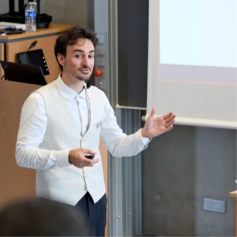
Thomas Harmand [ T.H. ]

Thomas Harmand

Co-Founder · PhD, Electrical Engineering

Thomas holds an M.S. in Electrical Engineering from INSA Lyon and earned his PhD in Power Electronics in June 2025 at the SATIE laboratory of ENS Paris-Saclay in industrial partnership with a leading European space-grade module manufacturer. His work focused on high-current, low-voltage output converters using GaN transistors for space applications, combining analog design with modern simulation tooling. After his thesis, he developed a commercial space-grade product and co-founded ADEV with Raphaël, pairing a research-driven approach with two decades of field-tested industrial expertise.

Raphaël Filipe [ R.F. ]

Raphaël Filipe

Co-Founder · Power Electronics Engineer

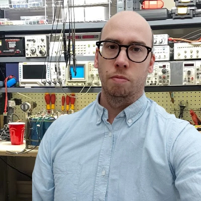
Raphaël is a seasoned power electronics expert with extensive experience in automotive and space applications. He holds an M.S. in Electrical Engineering from Polytech Paris-UPMC, Sorbonne University. His career spans Continental and Ausy, then 12 years at Valeo as electronic engineer and technical coordinator, followed by four years as Power Analog Electronic Design Expert in the space industry, leading the development of qualified DC-DC converters, an industrial track record that anchors ADEV's deliverables in real-world manufacturability.

0+ Years cumulative
experience
2025 Founded in
Palaiseau, France
0 Senior
partners
0% In-house engineering
and characterization

Have a hard problem?
Let's talk hardware.

Tell us about your project, topology, constraints, deadlines, and we'll come back with an honest technical assessment.

Based in France. We operate under NDA when required, confidentiality is standard practice, not an exception.

Loading question…

// 100% local check. No data sent to any third party.

We typically reply within one business day.

The information you provide is used solely to handle your request and is never shared with third parties. Learn more and exercise your rights in our Privacy Policy.